What is Glass Package Substrate?
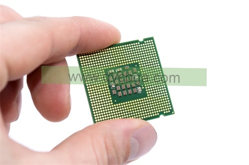
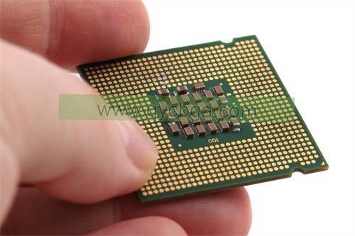
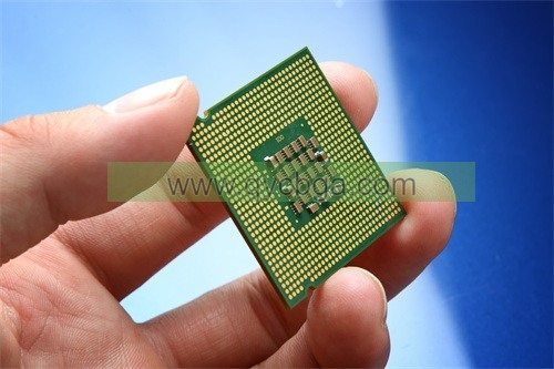
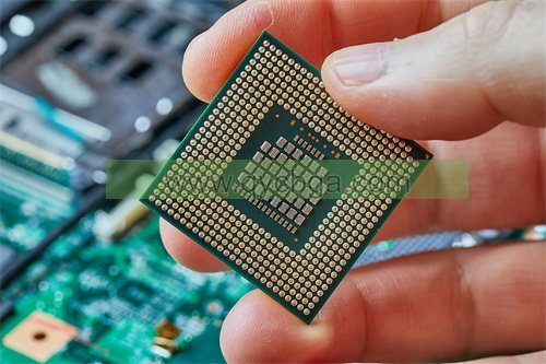
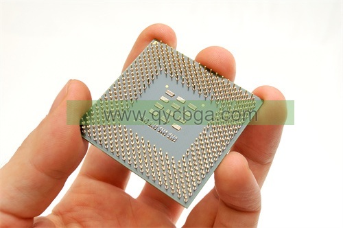
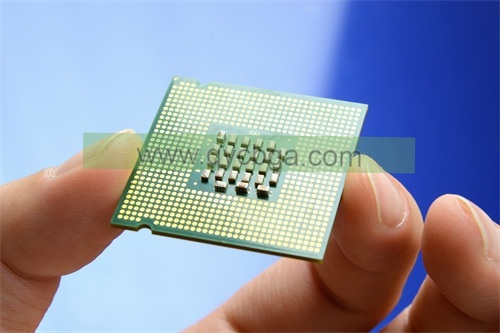
Glass Package Substrate Manufacturer,Glass package substrate is an emerging technology revolutionizing semiconductor packaging. Made from glass materials with advanced manufacturing techniques, it offers exceptional thermal stability, electrical insulation, and mechanical strength. Glass substrates provide high-density interconnects and precise routing capabilities, enhancing signal integrity and reliability. They are resistant to moisture, chemicals, and corrosion, making them ideal for harsh environments. Glass package substrates cater to various applications, including high-speed computing, telecommunications, and automotive electronics, where stringent performance requirements are critical. With their potential for miniaturization and superior performance, glass substrates pave the way for next-generation electronic devices with enhanced functionality and durability.
Glass Package Substrates (GPS) is a dedicated PCB that uses glass as the substrate material, unlike traditional materials such as FR-4. This innovative design brings many benefits, including higher thermal performance, improved reliability and enhanced signal integrity.
First, the thermal performance of glass substrates is far superior to traditional substrate materials. Due to the higher thermal conductivity of glass, GPS can more effectively transmit and dissipate the heat generated in the circuit, thereby reducing the operating temperature of components and extending the service life of the equipment.
Secondly, GPS has excellent reliability. Compared with traditional substrate materials, such as FR-4, glass substrates have higher mechanical and chemical stability and can better resist humidity, chemicals and mechanical stress, thereby improving the long-term stability and stability of electronic devices. reliability.
In addition, GPS provides excellent signal integrity. The low dielectric constant and low loss tangent of the glass substrate make it an ideal high-frequency circuit substrate, which can reduce signal attenuation and distortion during signal transmission and maintain signal accuracy and stability.
In general, glass packaging substrate, as a new type of PCB material, has broad application prospects in high-performance, high-reliability and high-frequency applications. Its unique advantages make it a favored choice in the electronic equipment manufacturing industry, promoting the continuous innovation and development of electronic products.

Glass Package Substrate Manufacturer
Glass Package Substrate design Reference Guide.
Design of a glass package substrate (GPS) involves steps similar to traditional PCB design, including schematic capture, component placement, routing and design verification. However, due to the unique characteristics of glass substrates, special attention must be paid to thermal management and signal integrity considerations.
First, the schematic capture phase is the starting point of the design process. At this stage, engineers will draw the logical structure of the circuit based on the device’s functional and performance requirements. Similar to traditional PCB design, use professional design software such as Altium Designer or KiCad to create a schematic, ensuring that all components are connected correctly and that the circuit structure meets specifications.
Next is component placement. At this stage, engineers will consider factors such as the size, shape and power consumption of the components, as well as how heat is conducted across the glass substrate. Because glass substrates conduct heat better, heat distribution across components can be more effectively managed, improving device performance and reliability.
Routing is one of the critical steps in the design process. At this stage, engineers need to consider the signal transmission path and impedance matching to ensure stable signal transmission in high-speed circuits. Compared with traditional PCB designs, routing on glass substrates may require smaller pitches and finer routing techniques to ensure signal integrity.
Finally, the design verification phase is critical to ensuring the accuracy and reliability of the GPS design. During this phase, engineers will use simulation tools and real-world testing to verify the performance and stability of the design. In particular, thermal management and signal integrity considerations require engineers to conduct exhaustive testing and analysis to ensure that the GPS design complies with specifications and meets the requirements of the device.
To summarize, designing a GPS involves a series of meticulous steps and special considerations, including thermal management and signal integrity. By following standardized design processes and using professional tools, engineers can design high-performance and reliable GPS to meet the requirements of various application scenarios.
What are the materials used in Glass Package Substrate?
Glass Package Substrates (GPS) mainly use glass as the substrate material, which has better thermal conductivity and mechanical stability than traditional substrates. The high thermal conductivity of glass substrates allows them to dissipate heat effectively, helping to improve the performance and reliability of electronic devices. In addition, the glass substrate has excellent mechanical stability and can maintain structural stability in complex environments, allowing it to maintain good working condition under high vibration and high temperature conditions.
In GPS, copper is used as a wire, responsible for transmitting electrical current and signals. Copper has good electrical conductivity and processability and can meet the needs of high-frequency and high-speed circuits. In addition, GPS may also use advanced dielectric materials to further enhance performance. These dielectric materials have low loss, high dielectric constant and excellent insulation properties, which help reduce losses in signal transmission and improve circuit stability and reliability.
Overall, GPS material selections are designed to achieve optimal thermal management, electrical performance and reliability. By utilizing glass substrates, copper wires and advanced dielectric materials, GPS can meet the high performance and reliability requirements of modern electronic equipment, providing important support for the development of the electronics industry.
How is Glass Package Substrate manufactured?
The glass package substrate (GPS) manufacturing process is similar to traditional PCBs, but additional steps are required to ensure the integrity of the glass substrate and optimize thermal performance.
First, the process of manufacturing a GPS begins with the preparation of the substrate. At this stage, the glass substrate is selected and surface treated to ensure the smooth progress of subsequent processes. Surface treatment can include cleaning, removing impurities and applying special coatings to enhance its heat resistance and adhesion.
Next comes the lamination of the glass layer. In this step, pre-processed glass sheets are pressed together to form a single glass substrate. This process requires precise control of temperature and pressure to ensure the quality and uniformity of the bond between the glass layers.
This is followed by the formation of the copper pattern. By covering copper foil on a glass substrate and using photolithography and etching techniques to define the circuit pattern. This step involves high-precision process control to ensure the precision and accuracy of the circuit pattern.
Next comes the etching process. By exposing the defined circuit pattern to a specific etching solution, the unwanted copper portions are gradually removed to form the desired circuit structure. This step requires strict process control to avoid quality problems caused by over-etching or under-etching.
Then comes drilling. High-precision drilling equipment is used to drill holes into the glass substrate that need to connect different layers of circuits. These holes are often called “vias,” and they allow electrical connections between circuit layers.
Finally, there is the surface treatment. Protect the circuit structure from the external environment by coating it with protective materials, such as solder paste or anti-corrosion agents. This step also includes final inspection and testing of the GPS to ensure its quality and performance meet design requirements.
In summary, the manufacturing process of GPS involves multiple key steps and requires precise process control and a high level of technical capabilities. Through these steps, glass packaging substrates with excellent performance and reliability can be produced, providing strong support for the development of modern electronic devices.
The Application area of Glass Package Substrate
Glass packaging substrate is a key component for electronic device packaging and has a variety of applications. The following are some of the main application areas for glass packaging substrates:
Smartphones and Tablets: In smartphones and tablets, glass packaging substrates are used as the basis for packaging and supporting chips and other electronic components. Due to its thinness, high strength and good thermal conductivity, glass packaging substrates can meet the miniaturization and high performance requirements of these devices.
TVs and Display Screens: In large-format TVs and displays, glass encapsulation substrates are used to support and encapsulate the electronic components required for display technologies such as liquid crystal displays (LCDs) and organic light-emitting diodes (OLEDs). Its highly flat surface and good optical properties make it ideal for display manufacturing.
Camera module: Glass packaging substrates play an important role in mobile phones and camera modules. They are used to support and protect camera sensors and lenses, while providing excellent optical properties to ensure image quality and sensor stability.
Automotive electronics: In the field of automotive electronics, glass packaging substrates are widely used in vehicle electronic equipment, such as vehicle infotainment systems, navigation systems, and driving assistance systems. Its high temperature resistance, vibration resistance and stable performance enable it to work reliably in harsh automotive environments.
Medical electronics: In medical electronic equipment, glass packaging substrates are often used to encapsulate and protect various sensors, circuits and display devices to ensure the reliability and stability of medical equipment. At the same time, its excellent biocompatibility also makes it one of the preferred materials for some medical sensors and equipment.
Industrial automation: In the field of industrial automation, glass packaging substrates are used to manufacture various sensors and controllers to realize monitoring, control and automation of factory equipment. Its corrosion resistance, anti-pollution and stable properties enable it to operate stably for a long time in harsh industrial environments.
Communication equipment: In communication equipment, glass packaging substrates are often used to encapsulate and protect key components such as radio frequency modules, antennas and optical devices to ensure the performance and stability of communication equipment. Its excellent electrical characteristics and high-frequency characteristics enable it to meet the requirements of communication equipment for high-speed transmission and high-frequency signal processing.
In general, glass packaging substrates play an important role in various electronic devices, and their excellent physical properties and engineering properties make them one of the key materials in the field of modern electronic packaging.
What are the advantages of Glass Package Substrate?
Glass Package Substrate is a new packaging technology with many advantages. Here are some of its advantages:
High reliability: Glass substrates have excellent mechanical properties and chemical stability, allowing them to maintain stability in a variety of environments. This enables glass packaging substrates to provide reliable performance under high temperatures, high humidity or harsh conditions.
Excellent thermal properties: Glass is an excellent insulating material with good thermal conductivity. This means that the glass packaging substrate can effectively dissipate heat and reduce the heat generated by the device during operation, thus improving the stability and reliability of the device.
Dimensional stability: Glass substrates have higher dimensional stability than traditional organic substrates. The glass packaging substrate is not prone to dimensional changes or warping due to temperature changes or long-term use, thus ensuring stable performance and appearance of the device.
Good optical properties: Glass substrates have good transparency and optical properties and can be used in some applications that require high optical performance, such as optoelectronic devices, display devices, etc.
Environmentally friendly and sustainable: Compared with some traditional packaging materials, glass substrates generally have better environmental performance and are recyclable, helping to reduce environmental impact.
High-density integration: The glass packaging substrate has high density and excellent flatness, which enables high-density integration of devices, thereby improving the performance and functionality of the device.
In general, glass packaging substrates have significant advantages in terms of high reliability, excellent thermal performance, dimensional stability, optical properties, environmental sustainability, and high-density integration. Therefore, they are used in some applications that require higher packaging technology. The field has broad application prospects.
How Much Does Glass Package Substrate Cost?
The cost of Glass Package Substrate (GPS) varies based on factors such as size, complexity and manufacturing volume. Generally speaking, the initial cost of GPS may be higher compared to traditional PCB. However, in terms of performance and reliability, the investment in GPS is often worth it in the long run.
First, the cost of a GPS is affected by its size. Larger size GPS usually requires more materials and production costs, so the price is relatively higher. At the same time, complexity is also a key factor affecting costs. If the GPS design requires complex wiring, high-density component layout, or special thermal management solutions, manufacturing costs may increase further.
In addition, manufacturing volume is also an important factor affecting the cost of GPS. Typically, larger production volumes can lead to lower unit prices because manufacturers can reduce unit costs through mass production. Conversely, small batch production may result in higher unit prices.
Although the initial cost of GPS may be higher, the performance and reliability benefits they provide often justify the investment in the long term. Because GPS have excellent thermal conductivity properties, improved reliability and enhanced signal integrity, they can reduce equipment failure rates, extend service life and improve performance. So while the investment cost of GPS may be higher, the long-term benefits in performance and reliability often outweigh the initial cost, making it an option worth considering.
FAQs
Can GPS be used in high-frequency applications?
Absolutely! One of the remarkable qualities of Glass Package Substrates (GPS) is their excellent performance in high-frequency applications. Due to their superior signal integrity characteristics and low dielectric loss, GPS are well-suited for a wide range of high-frequency applications, including wireless communication systems, radar technology, and microwave devices. The inherent properties of glass substrates, such as low loss tangent and stable dielectric constant, make them an ideal choice for maintaining signal integrity and minimizing electromagnetic interference (EMI) in demanding high-frequency environments.
What are the primary benefits of using glass substrates in PCB design?
The benefits of utilizing glass substrates in PCB design are manifold. Firstly, glass offers exceptional thermal conductivity, allowing for efficient heat dissipation and enhanced reliability, especially in applications with high-power components or operating in harsh environments. Additionally, glass substrates provide excellent mechanical stability and dimensional accuracy, reducing the risk of warping or deformation over time. Furthermore, the smooth surface of glass allows for precise patterning of fine traces and microvias, enabling high-density interconnects and miniaturization of electronic devices. Overall, the use of glass substrates in PCB design results in improved performance, reliability, and longevity of electronic products.
Are there any limitations or challenges associated with GPS design and manufacturing?
While Glass Package Substrates (GPS) offer numerous advantages, they may present certain challenges in design and manufacturing. One significant challenge is the handling and processing of glass substrates, which require specialized equipment and expertise to ensure proper handling and prevent breakage. Additionally, the cost of glass substrates may be higher compared to traditional materials like FR-4, potentially impacting the overall manufacturing cost of PCBs. Furthermore, the integration of components onto glass substrates may require modifications to standard assembly processes, necessitating collaboration between PCB designers and manufacturers to optimize manufacturing efficiency and yield. Despite these challenges, the benefits of using GPS in terms of performance, reliability, and signal integrity often outweigh the associated complexities, making them a preferred choice for advanced electronic applications.
Can GPS be used in harsh environments?
Yes, one of the key advantages of Glass Package Substrates (GPS) is their resilience in harsh environments. The use of glass as a substrate material offers superior mechanical stability and resistance to temperature extremes, making GPS ideal for applications in aerospace, automotive, and industrial settings where reliability is paramount.
Are GPS more expensive than traditional PCBs?
While GPS may have a higher initial cost compared to traditional PCBs, it’s essential to consider the long-term benefits they offer. Improved thermal performance, enhanced reliability, and superior signal integrity can result in cost savings over the lifecycle of electronic devices. Additionally, advancements in manufacturing technology are gradually reducing the cost gap between GPS and traditional PCBs.
What design considerations are unique to GPS?
Designing with Glass Package Substrates (GPS) requires careful consideration of thermal management and signal integrity. The high thermal conductivity of glass necessitates efficient heat dissipation strategies to prevent overheating and ensure component reliability. Signal integrity considerations include minimizing signal loss and electromagnetic interference (EMI) to maintain optimal performance in high-speed and high-frequency applications.
 FCBGA Package Substrate manufacturer

