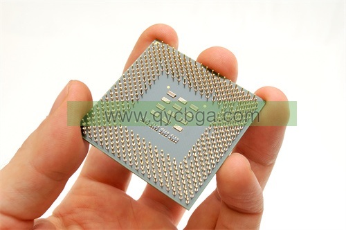
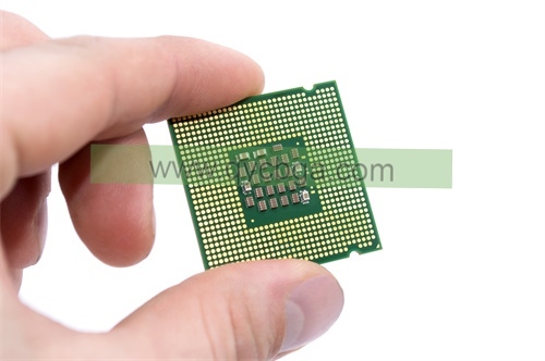
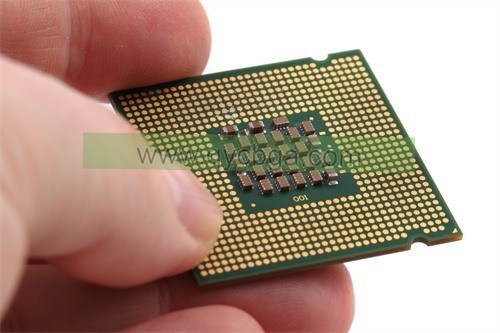
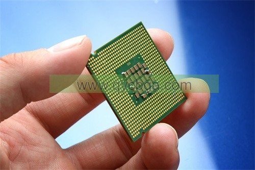
What is POP Package Substrate?
POP Package Substrate Manufacturer,PoP (Package on Package) package substrate is a sophisticated packaging technology designed to stack multiple semiconductor packages vertically. This configuration saves significant space and enhances performance by reducing the interconnect length between different functional components such as processors and memory. PoP substrates provide an efficient means for 3D integration, optimizing board space and enabling higher bandwidth through shorter interconnections. They are particularly beneficial in mobile devices, gaming consoles, and other consumer electronics where space is at a premium and high-speed operation is crucial. By facilitating tight integration and improved electrical performance, PoP package substrates play a crucial role in the development of compact, high-performance electronic products.
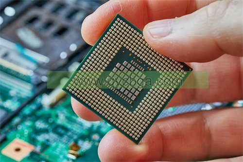
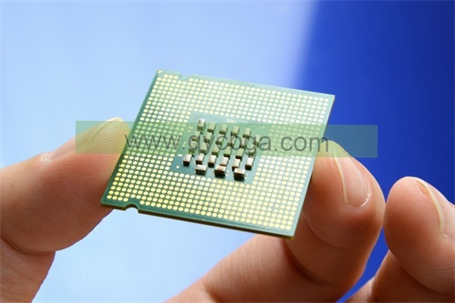
POP (Package-on-Package) substrate is a type of advanced packaging technology used in integrated circuits (ICs) and microelectronics. It involves stacking multiple chips or dies vertically on top of each other within a single package, which allows for increased functionality and performance in a smaller footprint.
In a POP configuration, one chip (typically a memory chip like DRAM) is mounted directly on top of another chip (usually a logic chip like a microprocessor or application-specific integrated circuit). This configuration enables various advantages such as reduced interconnect lengths between chips, which can lead to faster signal transmission and lower power consumption. It also allows for increased integration of different functionalities within a smaller form factor, which is especially important in mobile devices where space is limited.
The substrate in a POP package plays a crucial role in providing electrical connections between the stacked chips, managing heat dissipation, and providing mechanical support for the entire package. The substrate typically consists of a thin layer of insulating material (such as a laminate or organic substrate) with metal traces and vias that route signals between the chips and connect them to the external pins of the package.
Overall, POP technology has become increasingly important in the semiconductor industry, particularly in mobile devices like smartphones and tablets, where there is a constant demand for higher performance and functionality in smaller and more power-efficient form factors.

POP Package Substrate Manufacturer
POP Package Substrate design Reference Guide.
Designing a POP (Package-on-Package) substrate requires careful consideration of various factors to ensure optimal performance, reliability, and manufacturability. Here’s a reference guide outlining key aspects of POP package substrate design:
- Electrical Design: Ensure proper signal integrity by minimizing signal coupling and impedance mismatches. Route high-speed signal traces with controlled impedance to mitigate signal reflections and noise. Implement power distribution networks (PDNs) to deliver clean and stable power to the stacked chips.
- Thermal Management: Address heat dissipation challenges by incorporating thermal vias, thermal pads, or heat spreaders into the substrate design. Optimize the placement of components to facilitate efficient heat transfer and prevent thermal hotspots. Conduct thermal simulations to validate thermal performance under various operating conditions.
- Mechanical Considerations: Design the substrate to withstand mechanical stresses during handling, assembly, and operation. Specify appropriate material properties and thicknesses to achieve the desired mechanical strength and stiffness. Ensure compatibility with standard assembly processes such as flip-chip bonding and underfill encapsulation.
- Manufacturability: Design for manufacturability by adhering to industry-standard design rules and guidelines. Optimize the layout for ease of fabrication, assembly, and inspection. Consider the capabilities and limitations of the chosen manufacturing processes, such as photolithography, etching, and plating.
- Reliability Enhancement: Enhance reliability through proper design techniques such as minimizing solder joint stresses, optimizing solder mask coverage, and incorporating redundant signal paths where feasible. Perform reliability assessments using techniques like finite element analysis (FEA) and accelerated life testing (ALT) to identify and mitigate potential failure mechanisms.
- Signal and Power Integrity Analysis: Conduct thorough signal and power integrity analysis using simulation tools to predict and mitigate issues such as crosstalk, voltage droop, and timing violations. Verify the integrity of critical signals and power delivery networks under various operating conditions, including temperature extremes and voltage fluctuations.
- EMI/EMC Compliance: Design the substrate to minimize electromagnetic interference (EMI) emissions and ensure compliance with electromagnetic compatibility (EMC) standards. Employ proper shielding techniques, ground planes, and signal routing practices to mitigate EMI risks and enhance EMC performance.
- Documentation and Collaboration: Document the substrate design thoroughly, including schematic diagrams, layout files, design constraints, and manufacturing specifications. Collaborate closely with chip designers, assembly vendors, and testing partners to ensure alignment with overall system requirements and constraints.
By following these guidelines and best practices, designers can develop POP package substrates that meet the demanding performance, reliability, and manufacturability requirements of modern electronic devices.
What are the materials used in POP Package Substrate?
The materials used in a POP (Package-on-Package) substrate depend on several factors such as performance requirements, cost considerations, and manufacturing processes. However, common materials typically found in POP package substrates include:
- Organic Substrates: Organic substrates are commonly used in POP packages due to their excellent electrical properties, cost-effectiveness, and ease of manufacturing. These substrates are typically made from materials such as epoxy resin or polyimide, which provide good insulation and mechanical strength.
- Copper Foil: Copper foil is used to create conductive traces and vias on the substrate. Copper is preferred due to its high electrical conductivity and excellent solderability. Copper foils with different thicknesses may be used depending on the required current-carrying capacity and impedance control.
- Solder Mask: Solder mask is applied over the substrate to insulate and protect the copper traces from environmental factors and solder bridging during assembly. Solder mask materials are typically epoxy-based and are available in various colors, with green being the most common.
- Dielectric Materials: Dielectric materials are used to separate conductive layers and provide insulation between traces. Common dielectric materials include epoxy resin, polyimide, and cyanate ester. These materials offer high dielectric strength and thermal stability.
- Adhesive Materials: Adhesive materials are used to bond the stacked chips together within the package. These adhesives may be thermosetting or thermoplastic and are selected based on factors such as bonding strength, thermal conductivity, and compatibility with the substrate and chips.
- Solder Balls: Solder balls are used for chip-to-substrate and substrate-to-board interconnections in POP packages. These solder balls are typically made from a eutectic alloy such as tin-lead (SnPb) or lead-free alternatives like tin-silver-copper (SnAgCu) or tin-silver (SnAg).
- Encapsulation Materials: Encapsulation materials may be used to encapsulate the entire package for protection against moisture, mechanical shock, and other environmental factors. These materials are typically epoxy-based and are applied in liquid form before curing to form a solid encapsulant.
- Fillers and Reinforcements: Fillers and reinforcements may be added to the substrate material to enhance mechanical strength, thermal conductivity, or other properties. Common fillers include glass fibers, silica, and ceramic particles.
By carefully selecting and optimizing these materials, designers can create POP package substrates that meet the performance, reliability, and cost requirements of the target application.
How is POP Package Substrate manufactured?
Manufacturing a POP (Package-on-Package) substrate involves several steps to create a multi-layered substrate capable of supporting and interconnecting multiple chips within a single package. Here’s an overview of the typical manufacturing process:
- Substrate Fabrication: The process begins with the fabrication of the base substrate. This involves creating a thin layer of insulating material (such as epoxy resin or polyimide) and depositing copper foil on both sides. The copper foil is then patterned using photolithography and etching processes to create the desired conductive traces and vias.
- Layer Build-Up: Multiple layers of conductive traces and insulating dielectric materials are built up on the substrate to form a multi-layered structure. This is achieved through a series of steps including laminating alternating layers of copper foil and dielectric material, drilling vias, and plating the vias with copper to establish electrical connections between layers.
- Copper Plating and Etching: Copper plating is performed to thicken the conductive traces and fill the vias, ensuring low resistance electrical paths throughout the substrate. Excess copper is then removed through etching processes to define the final trace patterns and vias.
- Solder Mask Application: A solder mask layer is applied over the substrate to insulate and protect the copper traces from environmental factors and solder bridging during assembly. Solder mask materials are typically epoxy-based and are applied using screen printing or curtain coating techniques.
- Surface Finish: Surface finish processes are performed to ensure proper solderability and corrosion resistance of the substrate’s metal surfaces. Common surface finishes include immersion tin, immersion silver, electroless nickel immersion gold (ENIG), and organic solderability preservatives (OSP).
- Testing and Inspection: Various testing and inspection processes are conducted throughout the manufacturing process to ensure quality and reliability. This may include electrical continuity testing, impedance testing, dimensional inspection, and visual inspection for defects.
- Assembly: Once the substrate is manufactured, it is ready for chip assembly. This involves placing the individual chips (typically a logic chip and a memory chip) onto the substrate using flip-chip bonding or other appropriate bonding techniques. An adhesive may be applied to bond the chips to the substrate.
- Encapsulation: Optionally, the assembled chips and substrate may be encapsulated with a protective material (such as epoxy resin) to provide additional mechanical strength and environmental protection.
- Final Testing: The completed POP package undergoes final testing to ensure proper functionality and performance. This may include functional testing, electrical testing, thermal testing, and reliability testing to verify compliance with specifications and standards.
By following these manufacturing steps with precision and attention to detail, manufacturers can produce high-quality POP package substrates suitable for use in a wide range of electronic devices.
The Application area of POP Package Substrate
POP (Package-on-Package) substrates find applications in various electronic devices where space optimization, high performance, and compact form factors are essential. Some of the key application areas of POP package substrates include:
- Mobile Devices: POP technology is extensively used in smartphones, tablets, and wearable devices. By stacking memory chips (e.g., DRAM) on top of logic chips (e.g., microprocessors), POP packages enable manufacturers to achieve higher memory capacities and faster processing speeds within the limited space available in mobile devices.
- Consumer Electronics: POP substrates are also employed in a wide range of consumer electronics products such as digital cameras, portable media players, gaming consoles, and smart home devices. These applications benefit from the compact size, improved performance, and reduced power consumption offered by POP technology.
- Automotive Electronics: In automotive electronics, where space is often constrained and reliability is critical, POP packages are used in advanced driver assistance systems (ADAS), infotainment systems, navigation systems, and engine control units (ECUs). POP technology helps automotive manufacturers meet the stringent requirements for performance, durability, and miniaturization.
- Industrial Applications: Industrial equipment and machinery often utilize POP packages for processing units, data storage, and sensor interfaces. These applications require ruggedized electronics capable of withstanding harsh operating conditions, and POP substrates can provide the necessary performance and reliability in compact form factors.
- Networking and Communication Equipment: POP technology plays a vital role in networking and communication equipment such as routers, switches, base stations, and access points. By stacking multiple chips vertically, POP packages enable manufacturers to enhance data processing capabilities, improve network throughput, and reduce latency.
- Medical Devices: In medical devices and equipment, where reliability, miniaturization, and performance are critical, POP substrates are utilized in applications such as patient monitoring systems, diagnostic devices, imaging equipment, and implantable medical devices. POP technology enables the integration of advanced functionalities in smaller and more portable medical devices.
- Aerospace and Defense: Aerospace and defense applications demand high-performance electronics capable of operating in extreme environments with stringent reliability requirements. POP packages are used in avionics systems, satellite communication systems, radar systems, and military-grade electronics to meet these demanding specifications.
Overall, the versatility and benefits of POP package substrates make them suitable for a wide range of applications across various industries, contributing to the development of smaller, more powerful, and more energy-efficient electronic devices.
What are the advantages of POP Package Substrate?
Package-on-Package (POP) substrate technology offers several advantages that make it an attractive choice for integrated circuit packaging. Some of the key advantages of POP package substrates include:
- Space Savings: By vertically stacking multiple chips within a single package, POP technology enables significant space savings compared to traditional packaging methods. This compact form factor is especially beneficial in space-constrained applications such as mobile devices and wearable electronics.
- Increased Functionality: POP packages allow for the integration of multiple chips with different functionalities, such as a microprocessor and memory chips, within a single package. This integration enables devices to perform complex tasks more efficiently and supports advanced features and capabilities.
- Improved Performance: The short interconnect lengths between stacked chips in a POP package reduce signal propagation delays and enhance signal integrity, leading to improved overall performance. This results in faster data transfer rates, reduced latency, and enhanced system responsiveness.
- Enhanced Power Efficiency: POP technology can contribute to improved power efficiency by optimizing the placement of components and reducing parasitic capacitance and resistance in the interconnects. This enables devices to achieve longer battery life and lower power consumption, which is crucial for portable and battery-operated devices.
- Flexibility and Scalability: POP packages offer flexibility in design and scalability in terms of adding or upgrading components. Manufacturers can easily customize the configuration of stacked chips to meet specific application requirements and accommodate future technological advancements.
- Cost Effectiveness: While POP technology involves additional manufacturing complexity compared to traditional packaging methods, it can result in overall cost savings by reducing the need for additional components, simplifying assembly processes, and optimizing device designs for mass production.
- Improved Thermal Management: Stacking chips vertically in a POP package facilitates more efficient heat dissipation compared to side-by-side configurations. This helps prevent thermal issues such as overheating, which can degrade performance and reliability, especially in high-power applications.
- Reliability and Durability: POP packages typically undergo rigorous testing and qualification processes to ensure high reliability and durability. The stacked chip configuration can also provide mechanical stability and protection against environmental factors such as shock, vibration, and moisture.
Overall, the advantages of POP package substrates make them well-suited for a wide range of applications, including mobile devices, consumer electronics, automotive electronics, industrial equipment, and more, where space optimization, performance, and reliability are critical considerations.
How Much Does POP Package Substrate Cost?
The cost of POP (Package-on-Package) substrates can vary significantly depending on several factors, including the complexity of the design, the materials used, the manufacturing process, the volume of production, and market demand. Here are some key factors that influence the cost of POP package substrates:
- Design Complexity: The complexity of the POP substrate design, including the number of layers, the density of traces and vias, and the size of the substrate, can impact manufacturing costs. More complex designs may require specialized fabrication techniques and materials, leading to higher costs.
- Materials Used: The choice of materials for the substrate, such as organic substrates, copper foils, solder mask materials, and encapsulation materials, can affect the overall cost. High-quality materials with specific properties (e.g., high thermal conductivity, low dielectric constant) may be more expensive than standard materials.
- Manufacturing Process: The manufacturing process used to fabricate POP substrates, including photolithography, etching, plating, and assembly processes, can influence costs. Advanced manufacturing techniques and equipment may require higher upfront investments but can improve efficiency and reduce long-term production costs.
- Volume of Production: Economies of scale play a significant role in determining the cost of POP substrates. Higher volumes of production typically lead to lower per-unit costs due to optimized manufacturing processes, bulk material purchasing, and amortization of fixed costs over a larger number of units.
- Supplier Relationships: The relationship between the substrate manufacturer and suppliers of materials, equipment, and services can impact costs. Establishing long-term partnerships and negotiating favorable pricing terms may help reduce overall costs.
- Market Demand: Fluctuations in market demand for POP substrates can affect pricing dynamics. High demand may lead to increased competition among manufacturers, potentially driving prices down, while low demand may result in higher prices to cover fixed costs.
- Customization and Special Requirements: Customized features, special requirements, or additional testing and qualification processes may incur extra costs. These costs vary depending on the specific needs of the customer and the complexity of the customization.
It’s important to note that the cost of POP package substrates is typically determined on a case-by-case basis, taking into account all of the aforementioned factors. As such, it’s advisable for companies interested in utilizing POP technology to consult with substrate manufacturers to obtain accurate cost estimates based on their specific requirements and volumes.
FAQs about POP Package Substrate
What is a POP package substrate?
A POP package substrate is a type of advanced packaging technology used in integrated circuits (ICs) and microelectronics. It involves stacking multiple chips or dies vertically on top of each other within a single package.
What are the advantages of POP package substrates?
POP package substrates offer advantages such as space savings, increased functionality, improved performance, enhanced power efficiency, flexibility, scalability, cost-effectiveness, improved thermal management, and reliability.
What materials are used in POP package substrates?
Materials commonly used in POP package substrates include organic substrates (epoxy resin or polyimide), copper foil, solder mask materials, dielectric materials, adhesive materials, solder balls, encapsulation materials, fillers, and reinforcements.
How is a POP package substrate manufactured?
The manufacturing process for POP package substrates involves steps such as substrate fabrication, layer build-up, copper plating and etching, solder mask application, surface finish, testing and inspection, chip assembly, encapsulation (optional), and final testing.
What applications are POP package substrates used in?
POP package substrates find applications in various electronic devices and industries, including mobile devices, consumer electronics, automotive electronics, industrial applications, networking and communication equipment, medical devices, and aerospace and defense.
How much does a POP package substrate cost?
The cost of POP package substrates can vary depending on factors such as design complexity, materials used, manufacturing process, volume of production, supplier relationships, market demand, customization, and special requirements.
What are the considerations for designing a POP package substrate?
Key considerations for designing a POP package substrate include electrical design (signal integrity, power distribution), thermal management, mechanical considerations (mechanical strength, stiffness), manufacturability, reliability enhancement, signal and power integrity analysis, EMI/EMC compliance, documentation, and collaboration.
 FCBGA Package Substrate manufacturer

